
I recently found a video on the Applied Materials website that gives a breakdown on how a semiconductor is made (as seen here). At Intel, we used AMAT (Applied Materials) as the primary tool in the Fab. The area I worked in performed the CVD step. I worked with the Applied Centura HDP-CVD tool. HDP stands for High Density Plasma, and CVD stands for Chemical Vapor Deposition. In a CVD chamber a plasma cloud is established, the chemical reaction inside that cloud causes material to drift down and build up on the wafer, creating a thin film.
 note: we were depositing a fluorinated silicon dioxide film, not a diamond film (this was the best image I could find)
That layer of film was then manipulated by other steps to create the metal lines connecting the various layers of the microchip. What sets the HDP tool apart from basic CVD tools (or ones that only lay down an uniform thin film) is its ability to etch away at the film as it deposits it down. You might wonder why one would want to etch away at a film while it its being deposited, why not just create less film? HDP comes in when you consider the actual size of the metal lines used to interconnect the processor. While I was working at Intel, we were performing a .13 micron process, meaning the thickness of the metal lines are only .13 microns. Current generations are at .09 microns and .065 microns in the pipeline. The tricky part is, these metal lines leave an incredibly small gap between them. And when you try to lay a standard film from CVD on it, the holes do not fill completely. Think of it as if you have two houses very close together where the edges of the roofs are only about a foot apart. Now consider a huge snow storm. There will be a point where the gap between the roofs are decreased due to building snow, and the amount that ends up between the homes starts to get cut off. This is the basic principal of HDP, how do you ensure uniform filling of the small gaps between the metal lines? This is accomplished by etching and depositing at the same time. By cutting away at the edges of the metal lines, the space doesn't get cut off, and hence is filled correctly. Here is a picture of what the process ends up with:
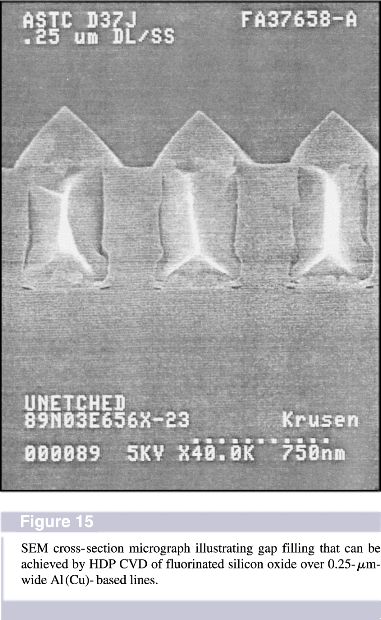 The three items in the middle are the metal lines, and the peaking of film on top is the result of etch/deposition. I think I'll close it up for now, don't want to bore you too much, and I should also note, the video from AMAT is a bit long. Enjoy

No comments:
Post a Comment